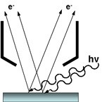
X-ray photoelectron spectroscopy (XPS), also known as ESCA (electron spectroscopy for chemical analysis) is a surface analysis technique which provides both elemental and chemical state information virtually without restriction on the type of material which can be analysed. It is a relatively simple technique where the sample is illuminated with X-rays which have enough energy to eject an electron from the atom. These ejected electrons are known as photoelectrons. The kinetic energy of these emitted electrons is characteristic of the element from which the photoelectron originated. The position and intensity of the peaks in an energy spectrum provide the desired chemical state and quantitative information. The surface sensitivity of XPS is determined by the distance that that photoelectron can travel through the material without losing any kinteic energy. These elastiaclly scattered photoelectrons contribute to the photoelectron peak, whilst photoelectrons that have been inelastically scattered, losing some kinetic energy before leaving the material, will contribute to the spectral background. The importance of surfaces in materials science is discussed in greater detail elsewhere
The chemical environment of an atom alters the binding energy (BE) of a photoelectron which results in a change in the measured kinetic energy (KE). The BE is related to the measured photoelectron KE by the simple equation; BE = hν - KE where hv is the photon (x-ray) energy. The chemical or bonding information of the element is derived from these chemical shifts.
Importance of energy resolution in XPS
XPS is a spectroscopic technique and therefore the energy resolution of the instrument is of fundamental importance. Energy resolution of an XPS instrument is usually measured as the full width at half-maximum (FWHM) of the Ag 3d5/2 peak. But is this useful?
The short answer is yes.
The longer answer is that the FWHM of the Ag 3d5/2 peak is a useful indication performance. It allows the ultimate energy resolution of instruments from different manufacturers to be compared. It also provides insight into the ability of the spectrometer to resolve, or separate, two closely spaced peaks in a photoelectron spectrum. Importantly, it doesn’t provide information on the peak intensity (counts per second). And therein lies the paradox of most spectroscopic techniques. As the energy resolution increases, the amount of signal collected decreases. So, to properly define the performance of an XPS instrument it is important to know the count rate at a given energy resolution.
What affects the energy resolution of my photoelectron spectrometer?
The easiest way to answer this is to understand what contributes to the measured peak width in an XPS spectrum. If we assume that the peak shape is the convolution of several Gaussian peaks, the measured peak width is given by:
Em2 = Ex2 + Elw2 + Einst2 equation 1
Where Em is the measured peak width, Ex is the width of the photon source, Elw is the natural line with of the electronic state being measured and Einst is the instrument resolution.
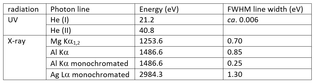
The commonly used excitation source for XPS experiments is monochromated Al Kα where Ex = 0.25 eV. The line widths of other excitation sources used on the AXIS spectrometers are shown in appendix 1.
As outlined above, the term Elw is the natural line width of the core-level that is being measured. This physical value will vary depending on the electronic energy level measured for the atom and the environment or chemical state of the atom within the material. Specifically, the natural line width is dominated by the lifetime broadening due to the core-hole lifetime of the excited state. In simple terms, this term contributes to the measured peak width as a consequence of the core level measured and the form of the material. For example, metal oxides typically have greater Elw than their elemental forms.
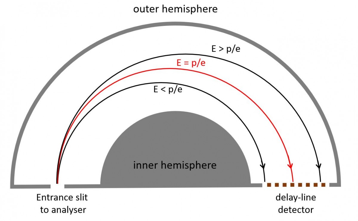
The final term considered is Einst and is the one that experimentalists have the most control over. The energy resolution of the instrument analyser is dependent on the chosen mode of operation, defined by the slit width used at the entrance to the analyser, the mean radius of the hemispheres, the angle of electrons entering the analyser at the entrance slit and the photoelectron pass energy. In practical terms most of the instrumental terms are defined by the manufacturer and the energy resolution is defined by the User in selecting the pass energy at which the data is collected.
The electron energy analyser is most commonly operated in fixed analyser transmission (FAT) mode. The photoelectrons are retarded to the selected pass energy, which is the mean kinetic energy of the photoelectrons as they move between the two hemispheres of the analyser. Operating in FAT mode has the advantage that energy resolution remains constant across the entire measured kinetic energy range. Selecting lower pass energy results in better the energy resolution of the collected photoelectrons at the cost of lower number of electrons being counted, or lower sensitivity.
Understanding the performance of the spectrometer and the information required from the sample defines how an XPS experiment is designed. The starting point for any XPS surface materials characterisation is a survey spectrum. It will provide a quantitative overview of the elemental composition of the sample. The survey spectrum is a low energy resolution, high sensitivity acquisition across the entire binding energy scale, typically 1200 to -5 eV. It is acquired at a high pass energy, for AXIS instruments this is 160 eV, and the step size is 1 eV. Acquiring data at 160 eV pass energy will give typical peak widths in the order of 3 to 4 eV. Under these acquisition conditions it will not be possible to determine chemical state information. But the spectrometer is in its most sensitive mode, so any trace, low concentration elements are most likely to be detected in this mode. High count rates associated with high pass energies mean that survey spectra can be collected inca. 60 seconds with excellent signal-to-noise.
To determine the chemistry of the sample the spectrometer must be operated at lower pass energy, typically 10 or 20 eV and acquisition step size of 0.1 eV for AXIS instruments. Narrow region, high resolution spectra are acquired from specific core-levels. Using these acquisition parameters, metallic core levels are typically < 0.6 eV. It is possible to determine chemical shifts caused by local chemical environment of the element being measured.
It is worth commenting on the effect the sample plays on the measured peak resolution. Insulating samples often have broader peaks due to longer core-hole lifetimes, such that Elw is the dominant term in equation 1 and the Einst does not limit the resolution of the acquired peak. In such a case, acquiring the narrow scan at 10 eV would not result in a narrower, higher energy resolution peak than one acquired at 20 or 40 eV. This physical effect is not limited to insulators, and many p, d and f core-level spectra are relatively broad and limit the ultimate peak resolution. A rough, topographic sample will have broader peaks than an atomically flat sample due to the scattering of photoelectrons as they leave the rough surface. Again, for such samples little or no improvement in energy resolution would be observed acquiring data at the lowest pass energies.
The skill of the spectroscopist is selecting the appropriate pass energy for the sample and analysis required. For AXIS instruments when acquiring ‘large area’ spectra a pass energy of 20 eV is found to be the best compromise between good energy resolution and enough signal for acquisition times to be between 60 – 300 s for a narrow region scan. Under these conditions polished Ag foil would have Ag 3d5/2 FWHM = 0.55 eV.
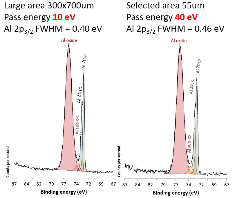
Effects of spectrometer configuration on energy resolution of the spectra can be explored using selected area spectroscopy for the AXIS instruments. To acquire spectra a fixed diameter aperture and variable diameter iris are used in the lens column of the spectrometer. A benefit of using this mechanism to define the small analysis area is that the spectroscopic resolution increases when compared to the large area (slot) analysis. By inserting the aperture and closing the iris, the trajectories of the photoelectrons are narrowed and there is less electron scattering in the analyser. This effect is more apparent for the smaller 27 um and 15 um analysis diameters.
For the experimentalist, the significance of this is that when using smaller analysis areas, it is possible to work at a higher pass energy and get similar energy resolution to the lower pass energies of large area mode. And, as stated, working at higher pass energy gives a higher sensitivity with the opportunity to reduce the acquisition time. These acquisition parameters also allow the ultimate energy resolution spectra to be acquired when required.
This is well demonstrated in the figure where the Al 2p region from aluminium foil was acquired from a large area (700x300 mm) at a pass energy of 10 eV where Al 2p3/2 FWHM = 0.40 eV, and a 55 mm diameter area at a pass energy of 40 eV where Al 2p3/2 FWHM = 0.46 eV.
Higher energy excitation sources (HAXPES)
In modern spectrometers the x-rays are energy filtered or monochromatised using a quartz crystal to give x-rays with very little energy spread. This monochromatic x-ray illumination of the sample enables high energy resolution of chemical shifts as well as detailed study of line profiles and subtle bonding changes evident in the valence band. There is growing interest in using higher energy X-ray excitation sources relative to the commonly used Al Kα (1486.6 eV) such as Ag Lα ( 2984.3 eV), Cr Kα (5414.9 eV) or Ga (9252 eV). One significant advantage of using higher energy photons is the ability to excite photoelectrons from higher binding energy core-levels. It is also the case that, with increased kinetic energy of core level electrons, the information depth also increases allowing greater sampling depth relative to conventional Al Kα. This is demonstrated by the increase in the information depth for Si 2p excited by Al Kα and Ag Lα which is 7 nm and 13 nm respectively [1].
Photoelectrons may also be collected from the surface in two dimensions to generate elemental or chemical state images of the surface.
The AXIS Supra+ spectrometers can be configured with XPS.
[1] M. P. Seah and W. A. Dench, Surf. Interface Anal. 1, 2 (1979)
Appendix 1
Natural line widths of excitation sources commonly used for photoemission spectroscopy experiments
[2] M.J. Edgell et al, Journal of Electron Spectroscopy and Related Phenomena, 37 (1985) 241-256