
In this article we will attempt to outline the importance of surfaces and X-ray photoelectron spectroscopy for materials science. But to be able to provide an answer to the question in the title, it is first necessary to ask ‘what is a surface’? In general terms surface can be described as the interface between two states of matter, typically a solid and a fluid. The physical properties of our solid include mechanical, thermal, electrical and optical and it is typically the bulk properties that define the use of that material for a specific application. However, it is the surface, or outermost layer of atoms of our solid that will really define how that material interacts with is surroundings and how it behaves for its intended purpose. In fact, the surface of our solid is perhaps the most important region of the material. For example, it will define adhesive properties. Will something stick to that surface such as a protective coating to prevent corrosion or reduce the ability of small cells to adhere and form biofilms? Can the surface chemical structure be modified to improve mechanical strength as is the case with super-hard coatings? There are many surface properties that materials scientists wish to manipulate to improve the functionality of the material. These surface properties include adhesion, conduction or insulation, optical transmission or reflection of electromagnetic radiation, hardness, (anti) friction or biocompatibility. The list is almost endless.
Thinking about surfaces within a mobile phone
As a consumer, probably the most important surface of your smart phone and the one that you interact with daily is the screen. The screen will be made of chemically strengthened glass, where the smaller sodium ions in the glass are exchanged by larger potassium ions. The larger ions create a surface layer of high residual compressive stress so that the glass has increased strength and crack-resistance. We also want the screen to be easy to clean, so it might typically be treated with a fluoropolymer, creating a hydrophobic surface which will also help improve its water repellencey.
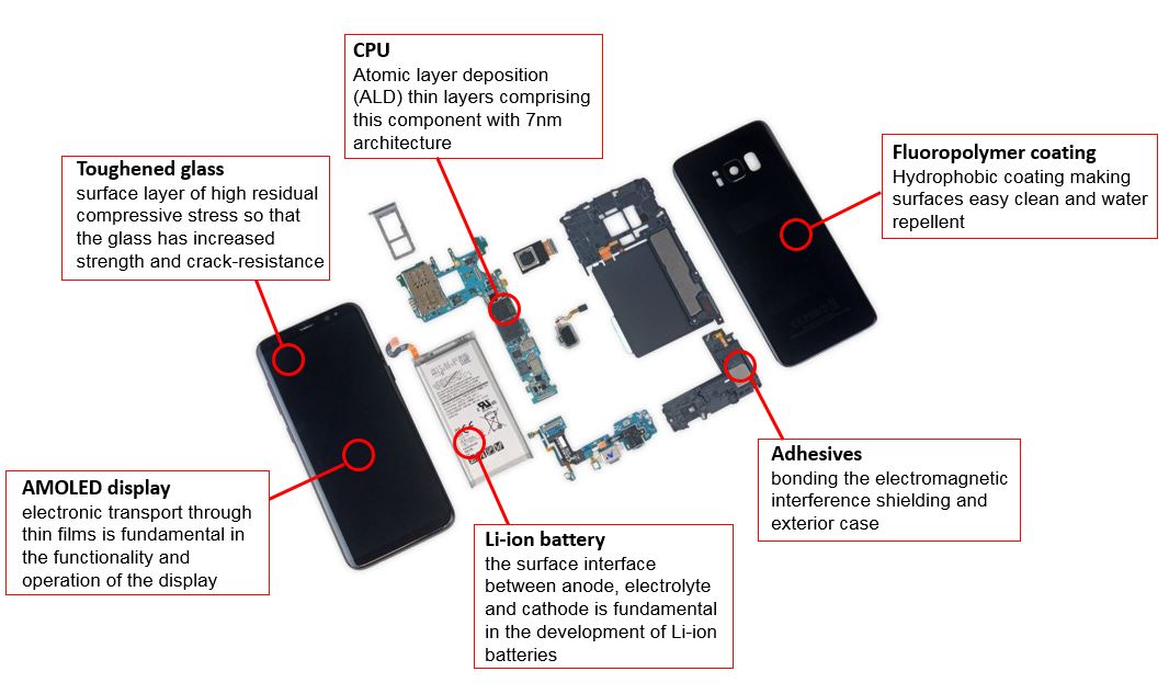
Another part of the phone that demonstrates the importance of surfaces is the display. Active matrix organic light emitting diode (AMOLED) displays are now common. The active matrix system attaches a thin film transistor (TFT) and capacitor to each LED where electronic transport through thin films are fundamental in the functionality and operation of the display.
The Li-ion battery is now ubiquitous but our expectation of longer battery lifetimes between charging and greater power demands of larger displays drive significant research into their improvement. The understanding of the surface interface between anode, electrolyte and cathode is fundamental in the development of Li-ion batteries.
When we start to consider our phone on a component by component basis, it is easy to begin to understand why surfaces are so important. The examples above are those that are perhaps most visible and therefore easy to highlight, but there are countless other examples; the electrical contacts to the packaged processor chip; the atomically deposited layers comprising the chip itself or the adhesive bonding the electromagnetic interference shielding and exterior case.
As the discipline of material science expands, so the development and application of novel materials expands. With it the requirement for fundamental understanding of surface chemistry increases. For example, in considering nanomaterials, as their size decreases, so the percentage of the surface relative to the bulk increases and will exert a greater influence on the properties of the material. Nanomaterials are being used in next generation products such as solar cells and display technology. It is perhaps the almost exponential growth in research and development of the ultimate nanomaterial, graphene and associated 2D materials, which are essentially a surface of single atoms that has thrown a spotlight on surface analysis applied to materials science.
The appliance of surface science
Having established that surfaces are fundamental in the performance of modern materials, our attention turns to the techniques available for surface characterisation. To understand and develop new materials and surfaces properties we need techniques which will measure only the first few nanometers of the surface as opposed to several microns, or bulk material. The primary techniques used for surface analysis are X-ray photoelectron spectroscopy (XPS), sometimes also known as electron spectroscopy for chemical analysis (ESCA), time-of-flight secondary ion mass spectrometry (ToF-SIMS) and Auger electron spectroscopy (AES). Each of these three techniques provide slightly different, complementary, information but has in common that the information comes from the first few nanometers of the material.
It is the first of these techniques, XPS, which has been most widely used for surface characterisation since the first commercial instrument was sold by Kratos Analytical, then AEI, in 1969. There are many excellent texts available providing a wealth of detail on the technique to which the interested reader is referred. In brief XPS involves measuring the kinetic energy of the photoelectrons ejected from a surface due to irradiating that surface by X-rays. The number and characteristic energies of the photoelectrons give a measure of the amount and identification of elements present in the surface of the material. Measurable shifts of the photoelectron peak energy, also known as chemical shifts, allow the interpretation of the chemical environment of the element. With XPS we are getting quantitative, surface specific, chemical state information from our sample. This is exactly the information that is vital to the materials scientist in understanding its performance for its intended application. By tailoring the surface chemistry, the material can resist corrosion, refract optical light, promote adhesion or conduct electrons more efficiently for example.
It is interesting highlight that the surface sensitivity derives from the distance that the excited photoelectron can travel through the material without losing any of its Kinetic energy, rather than the penetration depth of the X-ray photons used as the excitation source. By changing the energy of the photon source it is possible to change surface sensitivity of the photoemission technique. For the standard excitation source of Al Kα X-rays, the sampling depth is generally accepted to be ca. 10nm. Using more energetic Ag Lα X-ray excitation the sampling depth increases to ca. 18 nm, although this will vary on the specific photoemission line measured. Conversely, using much lower He I ultraviolet radiation, the sampling depth is only 2 – 3 nm.
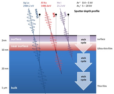
For thin-film characterisation it is sometimes necessary to combine XPS surface analysis with sputter depth profiling. Using either a monatomic Ar+ ion source or Arn+ cluster ion source to destructively remove material the elemental and even chemical composition can be determined as a function of depth from the original surface. Concentration depth profiles can be acquired up to several microns into the material when necessary.
Having considered the depth resolution of XPS it is also appropriate to consider the lateral resolution. A modern photoelectron spectrometer has a minimum sampling area of 10 – 15 um diameter which is perhaps where the complementary surface analysis techniques of ToF SIMS and AES have an advantage over XPS. It is noted that imaging XPS has an ultimate spatial resolution of 1 um and can acquire images of quantitative, chemical state distribution over fields of view of from 10 x 10 mm to 200 x 200 um. Combining XPS imaging and spectroscopy provides a powerful analytical technique for defect analysis.
Follow the links to read more about the capabilities of Kratos XPS instruments and applications of surface analysis across a broad range of modern materials.